Introduction
The Processor, which is a short alternative name of Microprocessor or often called as CPU (Central Processing Unit). CPU can be defined as the "brain" of a computer. CPU controls the computer. It is a part in a computer system that responsible to interpret and execute most commands from the computer program. It performs data processing operations such as arithmetic or logic operation, data manipulation tasks, logical and input/output of data. Processor only understands the instructions and it will follow the program's orders. It is the most important part of a computer. The difference of a good processor between a bad processor can be varied to their speeds, performances, graphics and multi-tasking abilities. Since processors can get heat very easily, so it always designed by attaching to the heat sink and fan in order to disperse heat from it. Nowadays, Intel and AMD branded processors are 2 of the most well-known processor in the world.How it works?
For example, when you double click an icon on desktop, a program will
be run. The program that stored in hard disk driver transferred to the RAM
memory. A program is a series of ordered instructions that allow computer to do
specific task. Then, RAM will stores info about the running program. The CPU
will load the program data from RAM by using the memory controller. Now the
program data have been processed inside a CPU. The CPU will follow the instructions
of the program to continue loading and executing data.
__________________________________________
A Sight inside the Processor
From the introduction, we know that CPU reads instruction from memory
(register, cache, main memory) so the CPU is necessary to keep some data for temporarily
as it has to store data temporarily in a small single read-write memory when a
command has been initiated. The instruction is decoded to determine what action
is required. Execution of an instruction may require reading data from memory
or an I/O module and performing some arithmetic or logical operation on data to
process the data. Finally, the results of an execution may require writing data
to memory or an I/O module. The whole execution will occur in sequential
manners from an instruction to another.
Figure 1.1.1 The sequence for a CPU to interpret and execute a command.
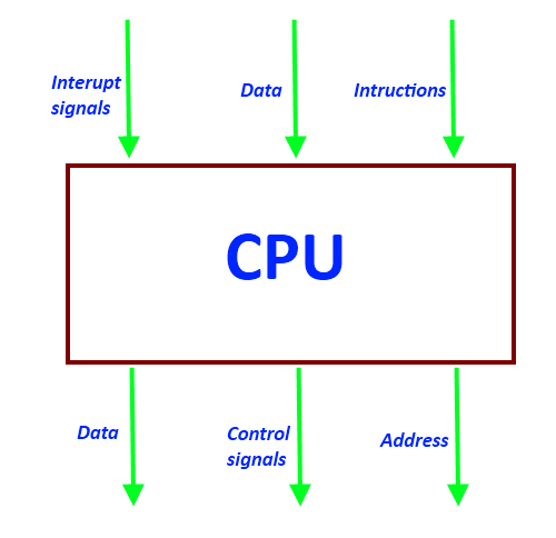
Figure 1.1.2 The movement for a CPU to interpret and execute a command.
When CPU reads instructions and data, then process the data and writes
it out. It will use control signals to control the entire operation of computer
system and receive interrupt signals. Control signals that generated for the
system bus such as the READ, WRITE and IO/M signals. By outputting the proper
signals in sequence, the control unit acts an important role to cause CPU fetch,
decode and execute every command in its instruction set properly.
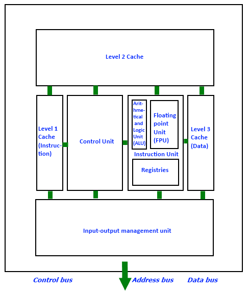
Figure 1.1.3 A simple CPU's internal organization
A CPU designed by considering all aspects of operation in software and
hardware based on levels of abstraction (levels of program codes) as below:
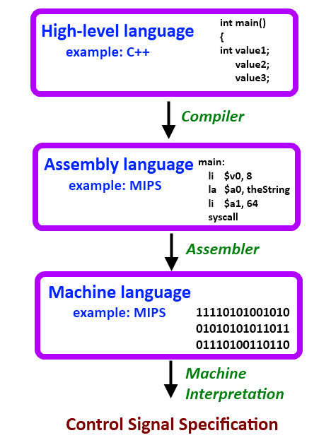
Figure 1.1.4 Levels of program codes for CPU
Reference:
1. http://en.wikipedia.org/wiki/Processor
2. Books:Computer Organisation and Architecture-8th Edition by William Stallings
by CSY
Processor Registers
IntroductionEvery processor has a local storage area known as a register that performs most of the operations that the processor cannot perform directly. Any kind of data must first be identified by the register before it can be manipulated by the processor. Processor registers are normally made of static or dynamic random access memory cells. Static RAM offers faster access to data than dynamic RAM .Computer system employs a memory hierarchy(a structure that use multiple levels of memories).Processor register at high levels of the memory hierarchy,memory is fast access to data,smaller and high speed of storage space.
Register Organization
Within the processor, there is a set of registers that function as a level of memory above main memory and cache in the hierarchy.The registers in the processor perform two rules:
Control and Status Registers
Control and Status Register (CSR) is a register in many central processing units that are used as storage devices for information about instructions received from machines. Most of these on machines are not visible to the user. Some of them may be visible to machine instructions executed in a control or operating system mode.
There are several types of registers. Example:
- Address registers - contain main memory addresses of data and instructions and used to store the addresses of other registers and different memory locations.
- Data registers - can be assigned to a variety of functions by the programmer and used to store intermediate data values and result when any arithmetic operation is performed.
- Conditional registers - hold truth values often used to determine whether some instruction should or should not be executed.
Types of register
Register is a sepecial memory used by the
CPU for temporarily storing data during execution of instruction.This are the
list of register types:
-Program counter (PC):It holds the
address of the next instruction to be executed。
-Instruction register (IR): It holds
the instruction being fetched
-Memory address register (MAR): It
holds address of a data word to be accessed
-Memory buffer register (MBR): It
holds the data word when it is transferred to and from the main memory
This above list of register types are used for the movement of data between the CPU and memory.
Typically, the CPU updates the PC after each instruction fetch so that the PC always points to the next instruction to be executed .The fetched instruction is loaded into an IR, where the operation code and operand specifiers are analyzed. Data are exchanged with memory using the MAR and MBR. In a bus-organized system, the MAR connects directly to the address bus, and the MBR connects directly to the data bus. User-visible registers, in turn, exchange data with the MBR. Many processor designs include a register or set of registers ,often know as program status word (PSW), that contain status information.The PSW typically
contains condition codes plus other status information.
Common fields or flags include the following:
- Sign: Contains the sign bit of the result of the last arithmetic operation.
- Zero: Set when the result is 0.
- Carry: Set if an operation resulted in a carry (addition) into or borrow (subtraction) out of a high-order hit. Used for multi-word arithmetic operations.
- Equal: Set if a logical compare result is equality.
- Overflow: Used to indicate arithmetic overflow.
- Interrupt enable/disable: Used to enable or disable interrupts.
- Supervisor: Indicates whether the CPU is executing in supervisor or user mode.
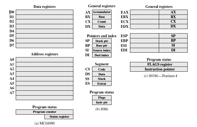
Example of Microprocessor Register Organizations.
Reference:
1. http://en.wikipedia.org/wiki/Processor_register
2. Books:Computer Organisation and Architecture-8th Edition by William Stallings-1
by Jian Tung
Instruction Cycle
An instruction cycle is the basic operation cycle of a computer.It is the process by which a computer retrieves a program instruction from its memory, determines what actions the instruction requires, and carries out those actions.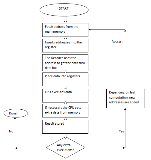
Figure 1.3.1 Instruction Cycle
There are 4 stages of an instruction cycle that the CPU carries out:
- Fetching the instruction
- Decode the instruction
- Read the effective address
- Execute the instruction

Figure 1.3.2 Stages of Instruction Cycle
Registers (small amount of storage available as part of CPU)
- Instruction Pointer (IP)
- The location of the next instruction
- Sometimes called the Program Center (PC)
- Memory Access Register (MAR)
- Current Instruction Register (CIR) or (IR)
- The current instruction
- Accumulator (AX)
- Used for short term storage, and in many instructions
- Memory Data Register (MDR)
The Fetch-Execute cycle in Transfer Notation
Expressed in register transfer notation:
MAR ß [PC]
MDR ß [Memory]MAR address; PC ß [PC]+1 (Increment the PC for next cycle at the same time)
IR ß [MDR]
Busses
- Address Bus
- Moves location of data to different registers, particularly between the Instruction Pointer, Memory Address Register and Memory.
- Data Bus
- Moves contents of memory addresses.
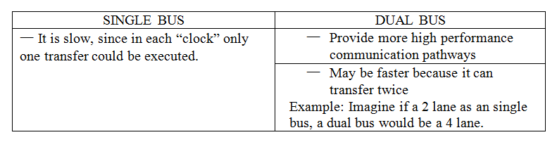
Figure 1.3.3 Comparison between Single Bus and Dual Bus
Reference:
1. http://en.wikipedia.org/wiki/Processor
2. Books:Computer Organisation and Architecture-8th Edition by William Stallings
By Kerrlyn
_______________________________________________________________________________________________
Instruction Pipelining
Pipelining enhance the number of instructions processed at 1 time.
Pipelining Strategy
Pipelining: new inputs are accepted before previous accepted inputs become outputs at the other end.
Instruction stage divide to 2 stages:
- FETCH instruction
- EXECUTE instruction
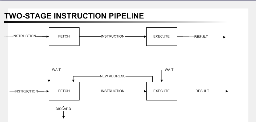
Figure 1.4.1 Stages of Instruction Pipelining
Second stage: when this stage executing instruction, first stage fetch and buffer next instruction. Fetch overlap/instruction prefetch occur.
Pipeline must have more stages to speedup:
- Fetch instruction (FI): read next expected instruction into buffer.
- Decode instruction (DI): to determine opcode, operand specifiers.
- Calculate operands (CO): calculate effective address of every source operand .
- Fetch operands (FO): fetch every operand from memory (except operands in registers).
- Execute instruction (EI): perform indicated operation, store result.
- Write operand (WO): store result in memory.
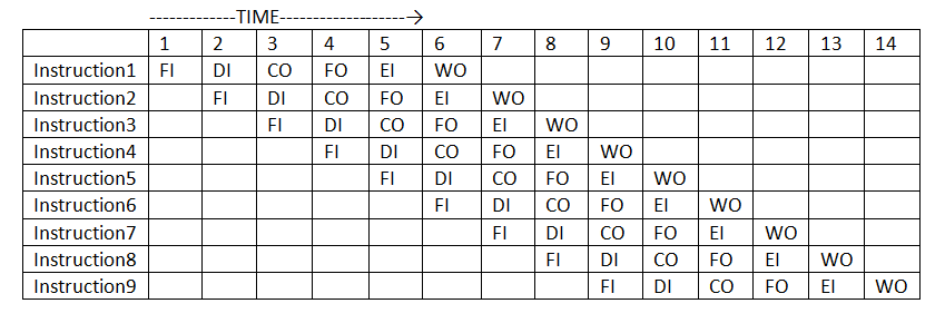
Figure 1.4.2 Timing Diagram For Instruction Pipelining Operation
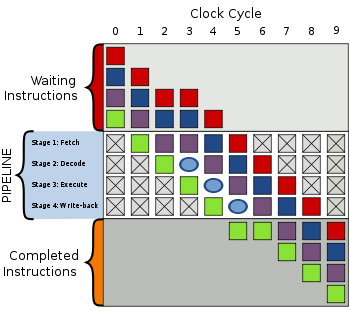
Figure 1.4.3 A Bubble in a Pipeline
Stalling and creating a bubble in pipeline is happened when pipelined processor may deal with hazards, this will cause one or more cycle and nothing useful happens. As an example, processor can’t decode purple instruction in cycle 3 it’s because processor determines decoding depends on results produce by execution of green instruction. Green instruction can proceed to next stage, which is Execute stage, then to Write-back stage,however,purple instruction stalled at Fetch stage for 1 cycle. Blue instruction also stalled for 1 cycle, it was due to be fetched during cycle 3. The processor's Decode circuitry is idle during cycle 3 because of bubble (illustrated in blue oval shape). During cycle 4 and cycle 5, Execute circuitry and Write-back circuitry are idle respectively. At cycle 6, the bubble moves out pipeline, and resume normal execution. All cycles are 1 cycle late, it won’t take 7 cycles but 8 cycles to execute 4 instructions as shown in picture above.
Pipeline Performance
To calculate cycle time:
T=maxi[Ti]+d= Tm+d 1
≤ i ≤ k
Where
T=Time delay of circuitry in ith stage of
pipeline
Tm=Maximum stage
delay
k=number of
stages in instruction pipeline
d=time delay of a latch,needed to advance signals and data from 1 stage
to the next
generally,d equivalent
to a clock pulse, Tm>>d.suppose n instructions are processed with no branches.
Tk,,n=[ k+(n-1) ]T
Where
Tk,,n =total time required for a pipeline
Processor with equivalent functions but without pipeline, assume instruction cycle time = kt. Speedup factor for instruction pipeline compared to execution when absence of pipeline:
Sk= (T1,n )/ (T k,n )=(n k T)/{[k+(n-1)] T }=(nk)/[ k+(n-1)]
Pipeline Hazards
WHY pipeline hazard happened? It happened when some portion of pipeline or pipeline must stall, it’s because condition not allow continued execution. (Pipeline bubble)
Hazards can separate to 3 types:
- Resource hazards/Structural hazard:
- 2 instructions which already executed in pipeline need the same resource. Therefore instructions executed in serial for a part of pipeline.
- Data hazards:
- When access an operand location, a conflict occurred.
- Data hazards can divide into 3 types:
- True dependency/Read after write (RAW).
- Anti-dependency/Write after read (RAW).
- Output dependency/Write after write (RAW).
- Control hazards/Branch hazard:
- Pipeline make decision wrongly on a branch prediction, and then brings instructions into pipeline that must discarded subsequently.
Dealing with branches
To deal conditional branches, variety of approaches has been taken:
- Multiple streams
- Pre-fetch branch target
- Loop buffer
- Branch prediction
- Delayed branch
1. http://en.wikipedia.org/wiki/Instruction_pipeline
By Wan Bing
_______________________________________________________________________________________________
History of the Processor
1969: FOUR-PHASE SYSTEMS AL1
- Arithmetic and logic unit (AL1)
- Is an 8-bit bit slice chip
- Contained 8 registers .
- Designed by Lee Boysel.
- Before was a chip, but later it was called a microprocessor.
1971: PICO/GI PICO1/GI250
- Introduced by Pico Electronics and General Instrument (GI)
- This chip claimed to be one of the first microprocessors or microcontrollers having ROM, RAM and a RISC instruction set on-chip.
1971: INTEL 4004
- Was introduced on November 15
- Designed by Federico Faggin, Ted Hoff of Intel, Masatoshi Shima of Busicom
- Intel's first microprocessor.
- Ran at 108 kilohertz (108,000 hertz)
- Consists of 2,300 transistors
- Performed 60,000 operations per second (OPS)
- Addressed 640 bytes of memory
- Powered the Busicom calculator.
1972: INTEL 8008 (MCS-8)
- Introduced on April 1.
- Developed by Victor Poor and Harry Pyle of CTC, and Ted Hoff, Faggin, Stanley Mazor and Hal Feeney from Intel.
- More powerful than the 4004.
- consists of 3500 transistors
- clock speed was 0.5MHz
- One of the first computers,The Mark-8 used in 8008 was difficult to build, sustain and used.
1974: INTEL 8080
- Introduced on April 1974
- Developed by Faggin, Mazor and Masatoshi Shima
- Consists of 6000 transistors
- Became the brains of the computer.
1974:
- TEXAS INSTRUMENTS TMS1000
- NATIONAL SEMICONDUCTOR "PACE" 16BIT
- MOTOROLA 6800
- No I/O ports
- The clock speed was only 2 MHz
1975: MOTOROLA 6502
1976:
ZILOG Z80
INTEL 8085 , INTRODUCED ON MARCH 1976.
INTEL 8086 , INTRODUCED ON JUNE 8, 1976.
1977: INTEL 8085
- The first time that Von Neumann architecture was used.
- Consists of 6500 transistors.
1978: INTEL 8086
- Clock speed was 10 MHz.
- Developed by Stephen P. Morse and Bruce Ravenel.
- First used in the microcomputer Mycron 2000.
1979: INTEL 8088
- Released on July 1.
- Designed frequency was 10 MHz.
- A pivotal sale to IBM's new personal computer division made the 8088 the brains of IBM's new hit product——the IBM PC.
1979: MOTOROLA 68000
- A 8-bit processor
- Chosen as the processor for the AppleMacintosh.
1981: HP 32 BIT
1982: INTEL 80286
- Introduced February 1.
- The first Intel processor
- Could run all the software written for its predecessor. This software compatibility remains a hallmark of Intel's family of microprocessors.
1985: INTEL 80386
- Introduced on October 1985.
- Has 275,000 transistors (>100times of the original 4004).
- It was a 32-bit chip .
- It could run multiple programs at the same time.
1987: SPARC
- First introduced by Sun Microsystems.
- Clock speed is of 40 MHz
- Consists of 1.8 million transistors
1988: INTEL 80386SX
1989: INTEL 80486
- The first to offer a built-in math co-processor, which speeds up computing because it offloads complex math functions from the central processor.
1989: AMD486DX
1991: AM386
- Introduced by AMD in March.
- Had resemblance to Intel 80386 version x86
- Clock speed of 40 MHz
- Was a competitor to Intel
1993: INTEL PENTIUM
- Released on March 22.
- Had clock speed of 60 MHz 510-pin version and clock speed of 66 MHz 567-pin version.
- Consists of 3.1 million transistors.
- Allowed computers to more easily incorporate "real world" data such as speech, sound, handwriting and photographic images.
1995: INTEL PENTIUM PRO
- Introduced in November.
- First processor of the Pentium II series
- Clock speed of 200 MHz
- Designed to fuel 32-bit server and workstation applications,
- Enables fast computer-aided design, mechanical engineering and scientific computation
- Packaged together with a second speed-enhancing cache memory chip.
- Consists of about 5.5 million transistors.
1997: INTEL PENTIUM II
- Introduced on May 7.
- Consists of 7.5 million transistors.
- Clock speed might increased up to 450 MHz
- Which is designed specifically to process video, audio and graphics data efficiently.
- It was introduced in innovative Single Edge Contact (S.E.C) Cartridge
- Incorporated a high-speed cache memory chip that can help PC users for capturing, editing and share digital photos or videos efficiently with friends and family via the Internet.
- Other processors launched under this family:
- Klamath (233 and 266 MHz)
- Deschutes (333 MHz)
- Pentium II Overdrive (300 or 333 MHz)
- Tonga (First mobile Pentium II)
- Dixon (Considered to be the fastest Pentium II)
1998: INTEL PENTIUM II XEON
- Designed to meet the performance requirements of mid-range and higher servers and workstations.
- Can deliver unique processor products targeted for specific markets segments.
- Specifically designed for workstations and servers that utilize demanding business applications such as electronic and mechanical design automation, and Internet services Systems based on the processor can be configured to scale to four or eight processors and beyond.
1999: INTEL CELERON
- Released on January 4th.
- Clock speed of 366 MHz and 400 MHz.
- Designed for the value PC market segment.
- It provides consumers great performance at an exceptional price.
- It delivers excellent performance for uses such as gaming and educational software.
1999: INTEL PENTIUM III
- 500 MHz is released on February 26.
- 550 MHz is released on May 17.
- 600 MHz is released on August 2.
- 533B and 600B MHz is released on September 27.
- Coppermine series is first introduced on October 25.
- Features 70 new instructions--Internet Streaming SIMD extensions.
- Dramatically enhance the performance of advanced streaming audio, video imaging, speech recognition applications and 3-D.
- Enhance Internet experiences, allows users for browsing, storing and downloading.
- Incorporates 9.5 million transistors.
- Introduced using 0.25-micron technology.
1999: INTEL PENTIUM III XEON™
- Extends Intel's offerings to the workstation and server market segments, providing additional performance for e-Commerce applications and advanced business computing.
- Incorporate the Pentium III processor's 70 SIMD instructions, which enhance multimedia and streaming video applications.
- Speeds information from the system bus to the processor, significantly boosting performance.
- It is designed for systems with multiprocessor configurations.
1999: ATHLON
- June 23
- Built with 37 million transistors
- Clock speed of 800 MHz
- Released by AMD.
- First processors to reach 1 GHz speed.
2000: INTEL 533 MHZ CELERON
- Released on January 4th
- Released 66 MHz bus processor in the same time.
2000: INTEL PENTIUM 4
- Clock speed of 1.3 GHz to 3.08 GHz.
- Can create professional-quality movies.
- Can simultaneously run several multimedia applications while connected to the Internet.
- Debuted with 42 million transistors and circuit lines of 0.18 microns.
- Ran at initial speed of 1.5 gigahertz (1.5 billion hertz).
- Other processors which was under this family:
- Willamette: Clock speed of 1.4 and 1.5 GHz
- Northwood: Clock speed up to 2.2 GHz
- Pentium 4-M: Built for Mobile use with TDP of 35 watts
- Mobile Pentium 4: Increased bus speed of 33 MHz and for the use of laptop.
- Gallatin: Die of 130 nm and an added 2 MB level 3 cache
- Prescott: Die of 90 nm and speeds up processes hyper-threading
- Prescott 2M: Clock speed of 3.8 GHz and 90 nm process
- Cedar Mill: Die of 65 nm
2001: INTEL 800 MHZ CELERON
- Released 100 MHz bus processor in the same time.
2001: INTEL XEON
- Targeted for high-performance and mid-range, dual-processor workstations, dual and multi-processor server configurations
- Offers customers a choice of operating systems and applications, along with high performance at affordable prices.
- Expected to achieve performance increases between 30 and 90 percent over systems featuring Pentium III Xeon
- Based on the Intel NetBurst™ architecture, which is designed to deliver the processing power needed for advanced Internet technologies, video and audio applications, , and complex 3-D graphics.
2001: INTEL ITANIUM
- The first in a family of 64-bit products from Intel.
- Designed for high-end, enterprise-class servers and workstations
- Built from the ground up with an entirely new architecture based on Intel's Explicitly Parallel Instruction Computing (EPIC) design technology.
- Delivers world-class performance for the most demanding enterprise and high-performance computing applications, including large databases, e-Commerce security transactions and mechanical computer-aided engineering.
2002:INTEL CELERON 1.3 GHZ
- Released with 100 MHz bus and 256 kB of level 2 cache.
2002: INTEL ITANIUM 2
- The second member of the Itanium processor family, a line of enterprise-class processors.
- Brings outstanding performance and the volume economics of the Intel Architecture to the most technical computing applications ,data-intensive and business-critical.
- It provides leading performance for databases, computer-aided engineering, secure online transactions, and more.
2003: INTEL PENTIUM M
- Clock speed of 2.26 GHz
- Introduced in March.
- One of the components of Centrino™ mobile technology .Designed specifically for portable computing, with built-in wireless LAN capability and breakthrough mobile performance.
- Enables extended battery life and thinner, lighter mobile computers.
- Other processors under tis family :
- Banias: Clock speed of 1.7 GHz and TDP of 24.5 watts
- Dothan: Die of 90 nm and clock speed of 2.1 GHz
2006:
INTEL CORE2 DUO PROCESSOR E6320
- Released on April 22.
INTEL CORE2 DUO PROCESSOR E6300
- Released on July 27
2007:
INTEL CORE2 DUO PROCESSOR E4300
- Released on January 21
INTEL CORE2 DUO PROCESSOR E4400
- Released on April 22
INTEL CORE2 DUO PROCESSOR E4500
- Released on July 22
INTEL CORE2 DUO PROCESSOR E4600
- Released on October 21
2008:
INTEL CORE2 DUO PROCESSOR E4700
- Released on March 2
INTEL CORE 2 DUO E7200
- Released on April 20
INTEL CORE2 DUO PROCESSOR E7300
- Released on August 10
INTEL CORE2 DUO PROCESSOR E7400
- Released on October 19
2009:
INTEL CORE2 DUO PROCESSOR E7500
- Released on January 18
INTEL CORE2 DUO PROCESSOR E7600
- Released on May 31.
2011:
SANDY BRIDGE
- Clock speed is of 3.6 GHz
- Achieved 32-nanometer die manufacturing
- Consists of improved 256-bit/cycle ring bus connect that interconnects different parts of processors
- Series under this family:
- Pentium: Clock speed up to 3.0 GHz
- Celeron: Clock speed up to 3.0 GHz
- Core i3: Clock speed up to 2.5 GHz
- Core i5: Clock speed up to 3.4 GHz
- Core i7: Clock speed up to 3.3 GHz
- Core i7 Extreme: Clock speed up to 3.8 GHz
INTEL IVY BRIDGE
- Introduced on April 29
- Achieved 22-nanometer die manufacture
- Includes special support for PCI Express and better graphic.
- Clock speed of 3.80 GHz
Reference:
1. http://www.tayloredge.com/museum/processor/processorhistory.html 2. http://www.buzzle.com/articles/history-of-computer-processors.html 3. http://www.computerhope.com/history/processor.htm
1. http://www.tayloredge.com/museum/processor/processorhistory.html 2. http://www.buzzle.com/articles/history-of-computer-processors.html 3. http://www.computerhope.com/history/processor.htm
by Fong
Thanks for posting this up :) its very Easy for me to understand it.
ReplyDeleteThanks for posting this up :) its very Easy for me to understand it.
ReplyDeletecan see u all put a lot of effort for doing this...thanks for sharing
ReplyDeleteAn insightful overview! Exploring processor details is key for tech enthusiasts. Detailed insights on functionality and performance.
ReplyDelete